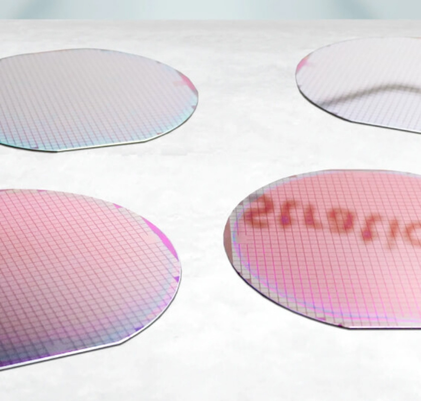
Wafer Fabrication
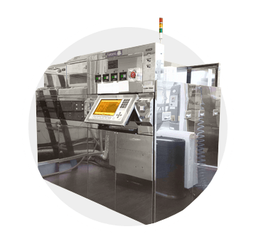
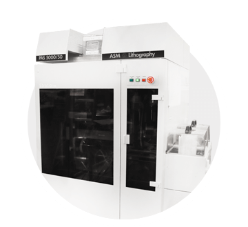
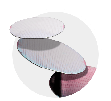
Custom wafer processes for sensors, MEMS and specialty semiconductors.


From wafer fabrication to packaging and multi-fab integration — all through one engineering partner.
Custom wafer processes for sensors, MEMS and specialty semiconductors.
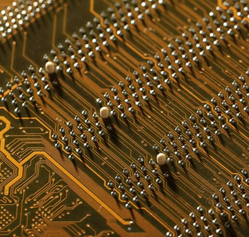
Wire bonding, chip bonding and device integration.
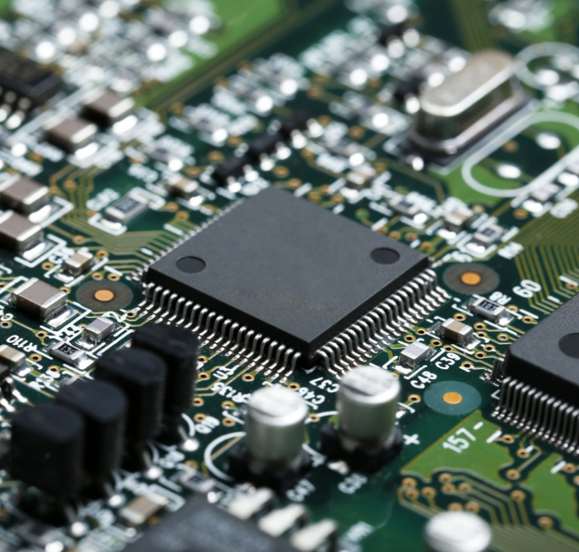
From bare die to functional prototype.
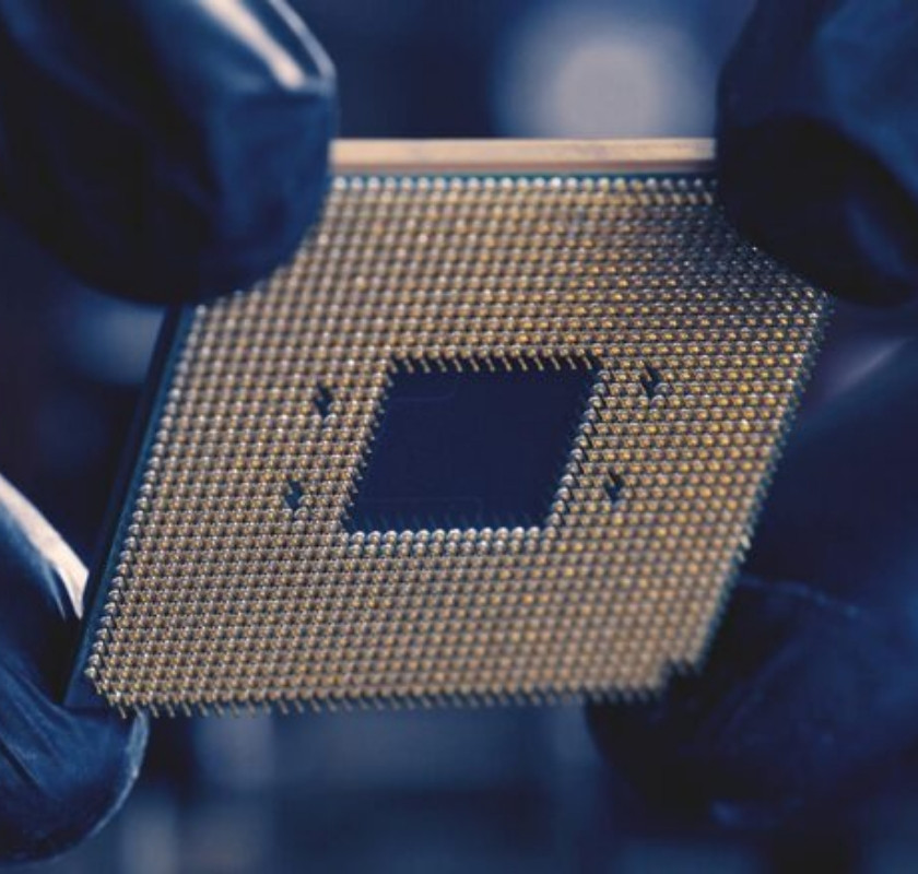
The right process. The right facility. One STNF interface.




















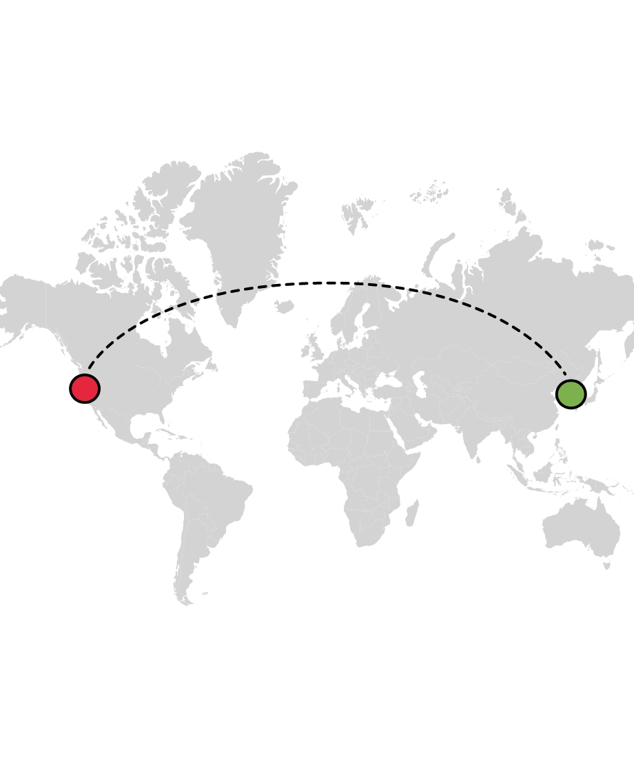
Connecting the right facilities across the U.S. and Korea for every process step.
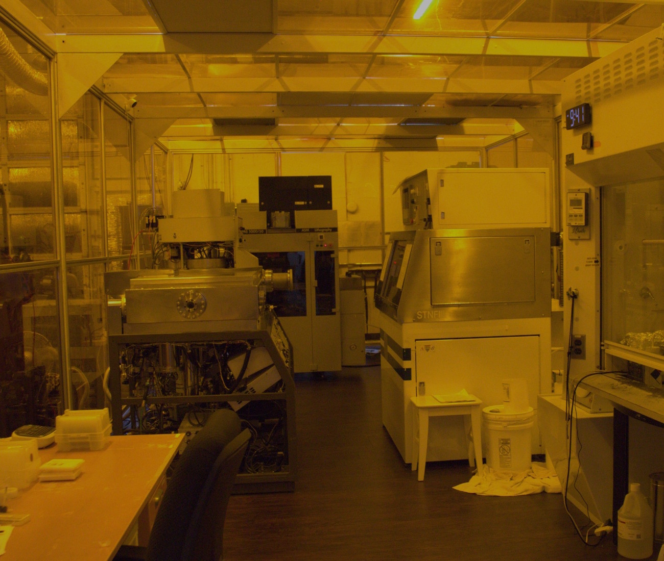
 United States
2211 Fortune Drive, Suite A, San Jose, CA 95131
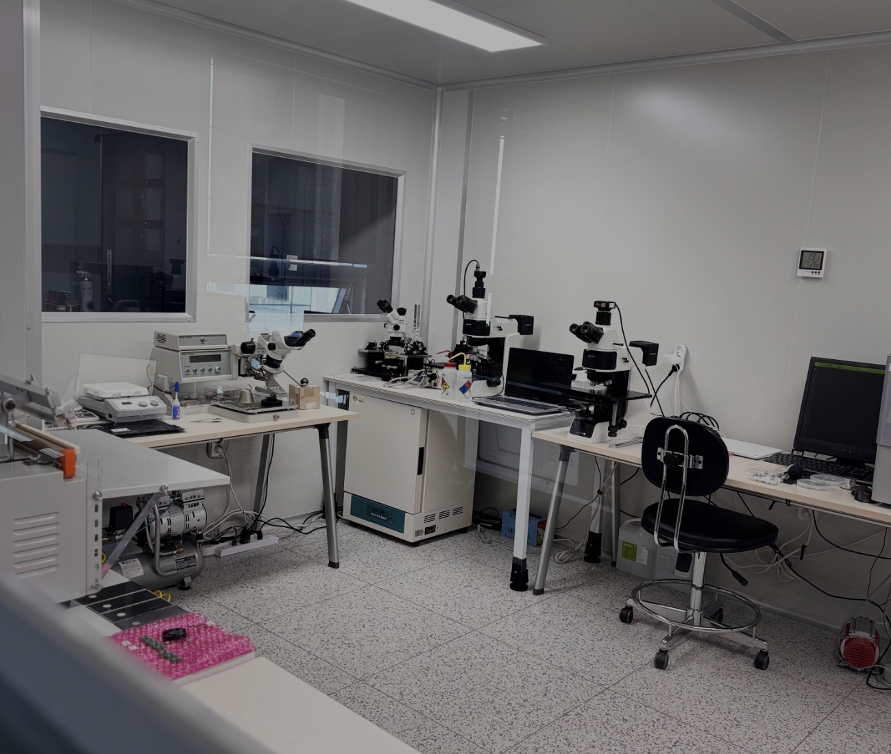
 South Korea
B-911, 43, Changeop-ro, Sujeong-gu, Seongnam-si, Gyeonggi-do (13449)
From wafer process to working device, STNF helps bring your semiconductor innovation to life.
Talk to our engineers