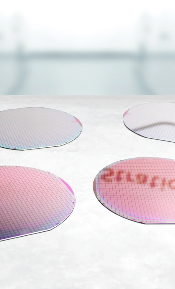
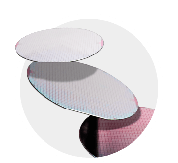
4-inch Nanofabrication Facility with CMOS & MEMS capabilities
At STNF, you can build your own readout integrated circuit
(ROIC) with 500 nm
technology nodes around your exiting invention or idea.
Our sensor foundry services
for ROIC/CMOS processes start at US$ 35K for one batch and
customers can reduce
the cost per wafer as they increase the batch size
At our 4-inch nanofabrication facility, we offer a
comprehensive range of wafer
fabrication processes- from Lithography, Etchning, Ashing,
to Chemical Mechanical
Polishing (CMP). Specializing in 4" wafers, we can also
process 4" downsized wafers
obtained via wafer coring. Striving to be a one-stop
solution provider, we also offer
PCB wire bonding services and keep a Scanning Electron
Microscope (SEM) available to
inspect customer samples.
The STNF team boasts a combined experience of 20+ years in
fabricating micro and nano
technologies in both CMOS and MEMS. Our journey began
within the walls of the Stanford
Nanofabrication Facility (SNF) and is now continuing at
our own in-house fab in San Jose.
As a consultant for SNF, we also provide consultation
services for device fabrication
as well as seamless transition into and out of working
with SNF.
At STNF, you can build your own readout integrated circuit (ROIC) with 500 nm technology nodes around your exiting invention or idea. Our sensor foundry services for ROIC/CMOS processes start at US$ 35K for one batch and customers can reduce the cost per wafer as they increase the batch size
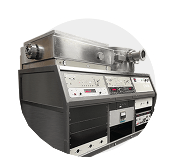
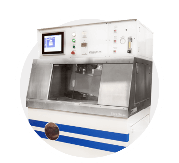
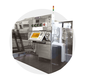
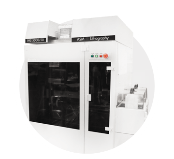
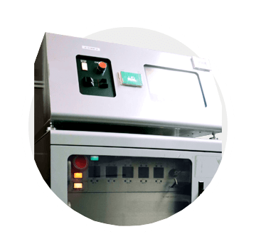
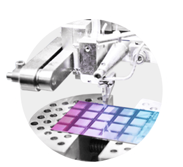
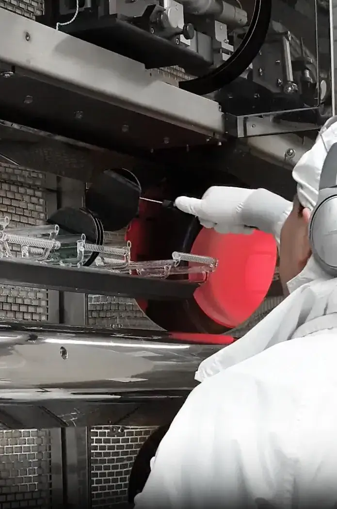
At our 4-inch nanofabrication facility, we offer a comprehensive range of wafer fabrication processes- from Lithography, Etchning, Ashing, to Chemical Mechanical Polishing (CMP). Specializing in 4" wafers, we can also process 4" downsized wafers obtained via wafer coring. Striving to be a one-stop solution provider, we also offer PCB wire bonding services and keep a Scanning Electron Microscope (SEM) available to inspect customer samples.
The STNF team boasts a combined experience of 20+ years in fabricating micro and nano technologies in both CMOS and MEMS. Our journey began within the walls of the Stanford Nanofabrication Facility (SNF) and is now continuing at our own in-house fab in San Jose. As a consultant for SNF, we also provide consultation services for device fabrication as well as seamless transition into and out of working with SNF.
At our 4 inch nanofabrication facility, a comprehensive
range
of wafer fabrication processes is at your service - from
Lithography,
Etchning, Ashing, to Chemical Mechanical Polishing
(CMP).
Specialized in 4" wafers, we can also process 4" downsized
wafers
obtained via wafer coring. Striving to be a one-stop
solution provider,
we also offer PCB wire bonding services and keep a
Scanning Electron Microscope (SEM)
available to inspect your samples.
The STNF team has a combined experience of 20 years in
fabricating
micro and nano technologies, beginning from within
the walls
of Stanford Nanofabrication Facility (SNF)
and now
continuing in San Jose at our in-house fab.
As a consultant of SNF, we also provide consultation
services
for device fabrication as well as seamless transition
into and out of SNF.
PROCESS CAPABILITIES (INCLUDING SNF CONSULTING)
Chosen by
We Care About Our Customers


HISTORY
STNF was created by STRATIO, INC. as a part of our journey
to bring infrared
vision to the mass market through our smart infrared
devices LinkSquare® and
BeyonSense®. Originating from our experience in building
these novel devices
with in-house resources, STNF has acquired its own
cleanroom facilities to
ensure control over quality and efficiency in production.
STNF, a 4" fab in the San Francisco Bay area, was first
opened to the public
in 2020. This facility was designed to support the
development of our own
innovations as well as serve as a starting point for
others. Today we strive
to help others bring their own innovative ideas to
fruition and enable a better
world for the future.
HISTORY
The Stratio Technology Nanofabrication Facility (STNF)
is in San Jose, California, in proximity
to the
Stanford Nanofabrication Facility (SNF).
We are proud to be a part of the semiconductor tradition
at the heart of Silicon Valley and to carry
on the history of "made in California".